
Quantum sensing
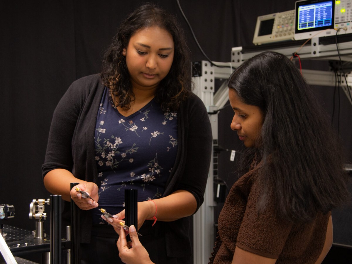
Quantum sensors harness quantum phenomena, such as superposition or entanglement, to measure magnetic and electric fields, strain, and temperature with sensitivity that can exceed classical limits. Crystallographic defects in solids are among the most promising platforms: their electron spins respond to their local environment and can, in principle, resolve features below a nanometer (Sushkov et al., 2014).
We develop quantum sensing techniques based on solid-state spin defects, with applications ranging from nanoscale magnetic resonance (Budakian et al., 2024; Du et al., 2024) to thermometry. Our goal is to translate these advances into practical, deployable sensors for chemistry, biology, clean energy, and beyond.
Solid-state qubits
Efficient spin–photon interfaces are the backbone of quantum sensors and networks. The ideal qubit combines bright, spectrally stable optical transitions with long-lived electron and nuclear spins.
We develop techniques to create near-surface defects in diamond (Rose et al., 2018; Harris et al., 2020; Thiering & Gali, 2021) and in alternative materials such as silicon (Higginbottom et al., 2022), and investigate their optical and spin properties to identify promising candidates for quantum technologies.
Quantum devices
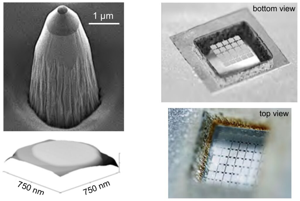
Nanofabricated structures control how quantum defects interact with light. We design photonic devices such as waveguides that efficiently collect emission from single defects (Zhu et al., 2023) and optical microcavities that enhance it (Zifkin et al., 2024). We are also developing fabrication processes in diamond and silicon, including in UCalgary’s upcoming QLab cleanroom.
These devices can boost the brightness and sensitivity of quantum sensors and provide building blocks for quantum communication technologies.